LASER DIRECT IMAGING (LDI) IN PCB MANUFACTURING
From: Author:smt pcb assembly line Publish time:2021-10-04 21:06 Clicks:0
In the world of PCB Manufacturing, it is important to stay as up-to-date as possible with industry trends. This is because, circuit boards are constantly evolving and getting more complex, due to miniaturization trends in the electronics industry. These changes have caused the traditional imaging process for HDI PCBs to provide inadequate results.
In response to new electronics tendencies, the PCB manufacturing industry has come up with a new imaging technique known as Laser Direct Imaging. Below you will find an introductory guide to this process.
WHAT EXACTLY IS LDI?
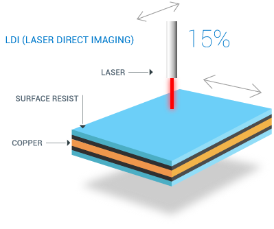
When a circuit board is made, the imaging process is what defines the circuit traces. While the traditional imaging process requires a photo-tool and UV-light to transfer images, LDI only uses a computer-controlled, highly focused, laser beam to directly define the circuit pattern onto the board.
HOW DOES LDI WORK?
This process can be summed up in the following steps:
- 1) The panel is coated with a layer of photoresist
- 2) The CAM files are preloaded into the laser.
- 3) The circuit pattern is digitally created onto the board by the CNC laser.
- 4) Using acid, the areas that weren't exposed to the laser beam are then etched, leaving intact the circuit traces.

WHAT ARE SOME ADVANTAGES OF USING LASER DIRECT IMAGING?
Using LDI to create the circuit traces gives the PCB manufacturers a lot of advantages, most of them pertaining to weaknesses of using a Photo-tool. Eliminating the need of a Photo-tool removes alignment issues, light refraction issues, and those imperfections related to environmental variations.
Also, with LDI, PCB factories can achieve the development of images that require more precision, and resolution, due to the computer's enhanced optical alignment, that automatically compensates distortion on the materials.
Changes to the required images, are also easier to achieve with LDI: with the traditional approach, the smallest mistake on the Photo-tool, required the factory to produce a new one, wasting time and money; however, with LDI, these changes became a matter of updating the design file, which can be done more consistently and cost-effectively.
Keywords:
SMT Line PCB, SMT Full Line, Dual Squeegee Semi-AutomatIC Stencil Printer, Desktop Stencil Printer SMT AutomatIC, Reflow Oven Profiler, Manual SMT Reflow Oven, Wave Soldering Machine Nozzle, Wave Soldering Machine With Flux, Hanwha PICk And Place PCB Machine, PICk And Place Machine 2 Head, Vaccume SMD PICk And Place Machine, SMD PICk And Place Machine, Vision Camera SMT PICk And Place, PanasonIC PICk And Place SplICing Tape, PICk And Place Machine For Packaging, DIP Capacitor PICk And Place Machinery, Conformal Coating Machine Selective, LED Shell AutomatIC Coating Line, PCBA Conformal Coating Line, Desktop PCB Router Machine, Router Power Backup PCB, CNC Router PCB Board, CNC PCB Router Drill
I.C.T is a manufacturer of SMT machines. It mainly provides customers with SMT production lines including SMT Stencil Printers, Pick and place machines, Reflow Oven, AOI Machine, Wave Soldering Machine and PCB Handling Machine etc. I.C.T has more than 25 researches on SMT and DIP technology, for the world Customers provide SMT total solutions. There are successful cases of SMT technical team in Asia, Europe, America, Africa, and Australia.
I.C.T provide SMT solutions at various stages according to the different needs of customers. I.C.T is not only a provider of SMT equipment and technology, but also is the customer's escort in the field of SMT and DIP.
Welcome more people to discuss with us about SMT technologies and solutions, please contact us for more information:
Tel: +86 13670124230 (WhatsApp/Skype/WeChat)
Email: etasmt@foxmail.com

