PCB X-ray
From: Author:PCB X-ray Publish time:2021-09-15 11:18 Clicks:0
Basic Description
The I.C.T-8200 is the latest version of the PCB X-ray inspection machine that I.C.T provided.
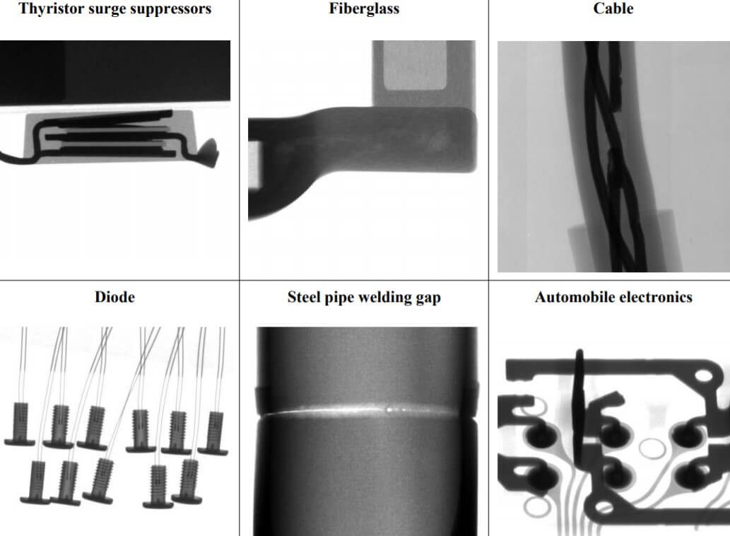
It adopts the Japan Hamamatsu X-ray source and Korea Rayence flat panel detector, which ensures high-accuracy of focal spot size and pixel size. As a result, a clear X-ray image is capable to be produced.
Besides, it has a large detection area of 530×530 millimeters, which meets the inspection requirement of big PCB boards.
What’s more, its software system is also highly intelligent and automatic. There are image effect adjustment method, display real-time coordination, movement speed control, void rate automatic calculation, etc.
Feature
Demonstration of PCB X-ray Application


1. Two Core Hardware Parts
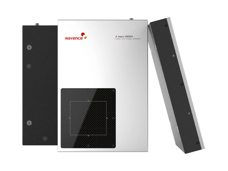
- Panel Detector(0505A) : Rayence has built the world’s first full line-up of dental, medical, veterinary, and industrial X-ray detector products. Also, in Korea, Rayence is the only company that owns the techniques for designing CMOS wafer, developing flat panel detectors (TFT), and using the core technology of scintillator, which is used for radiation detection.

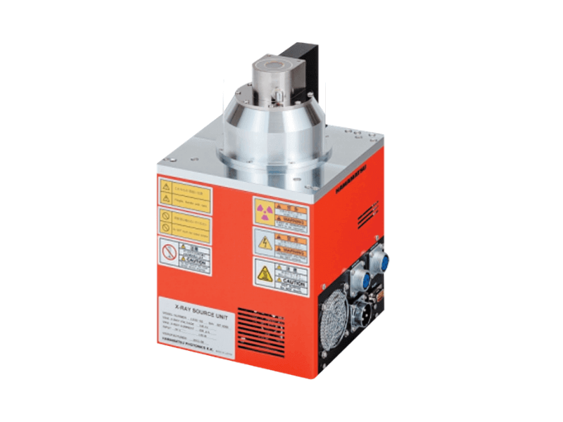
- Hamamatsu X-Ray Source(90KV) : The Hamamatsu microfocus X-ray sources have been evolved specifically for X-ray non-destructive inspection system. These X-ray sources equipped with an X-ray tube that has a small focal spot of several micro-meters to ten micro-meters, able to generating a clear X-ray picture even at a high magnification.
- The RS-232C interface is supplied as a widespread feature, permitting computerized operation with the aid of using outside control.
- The X-ray tube has an air-cooled and hermetically sealed structure, and is included with its excessive voltage electricity deliver for smooth handling. (High voltage cables are not required.)

2. Friendly Design of PCB Xray
- FPD instead of the table can tilt 60°, which won’t sacrifice magnification.
- The speed is adjustable, 5 axis coordination linkage system is adopted, which can maintain the image central while tilting.
- The speed is adjustable, 5 axis coordination linkage system is adopted, which can maintain the image central while tilting.
- The inspection procedures can be edited to achieve automatic inspection in large quantities.
3. Software Feature – Function Module
- Operation : Keyboard and mouse can finish all operations
- PCB X-ray Tube Control : Using mouse to click the X button can turn on or off the X-ray. The real-time tube voltage and current value will display beside, users can click up and down button, or drag the slider, or type to adjust.
- Image Effect Adjustment : The brightness, contrast and gain of the image can be adjusted freely to achieve a satisfactory result.
- Product List : Users can save the inspection parameters such as x-axis coordinates, contrast, brightness, and gain, and can directly call the parameters when inspecting the same product, to improve the inspection efficiency.
- Navigation Window : After the camera takes a photo of the table, click anywhere in the photo, the table will move to the place you click and display on the screen.
4. Software Feature – Void Rate Measurement
- Automatic Calculation : Click on two points to determine a rectangle. The software automatically finds and measures the edge of the solder ball in the rectangle, the pad and the internal voids, and can get the data of the voids rate, the area of the solder ball, the circumference, the biggest void’s rate, the length and the width, and indicates NG or OK by red and green
- Parameters Adjustment : Users can adjust the grayscale threshold, pixel, contrast, size filtering and other parameters to get accurate results of automatic calculation.
- Add Voids Manually : Users can draw a polygon or a free figure and calculate it as a void into the void rate.
5. Software Feature – Automatic Inspection
- Manual Setting : Users can set any positions on the table as inspection points, the software will automatically inspect and save the picture.
- Array : For the regular inspection points, users only need to set two of the inspection points and the number of rows and columns, the software will automatically inspect each point and save pictures.
- Automatic Identification : For inspection points with obvious features, the software automatically identifies the positions, takes measurements, and saves the image.
Keywords:
Small SMT Production Line, SMT Line Input Conveyor, Small Stencil Printer, Stencil Paste Printer, SMT Reflow Soldering Oven, Reflow Oven Heating, Wave Soldering Machine PrICe, SMT PICk And Place Head, PICk And Place Machine A9, PICk And Place IC Handler, PICk And Place Machine Sm482Plus, Gsm PICk And Place Nozels, Capacitor PICk And Place Machinery, Semi AutomatIC PICk And Place, PICk And Place Machine Kit, Small PICk And Place PneumatIC, PCB Magazine Loader, SMT Conveyor, SMT Conveyor System, Auto PCB Loader, PCB VertICal Loader, SMT Unloader Peripheral, SMT PCB Loader, Board Stacker Conveyor, PCB Manual RoutewrPCB Manual Router, PCB Router Machine Circuit Board
I.C.T is a manufacturer of SMT machines. It mainly provides customers with SMT production lines including SMT Stencil Printers, Pick and place machines, Reflow Oven, AOI Machine, Wave Soldering Machine and PCB Handling Machine etc. I.C.T has more than 25 researches on SMT and DIP technology, for the world Customers provide SMT total solutions. There are successful cases of SMT technical team in Asia, Europe, America, Africa, and Australia.
I.C.T provide SMT solutions at various stages according to the different needs of customers. I.C.T is not only a provider of SMT equipment and technology, but also is the customer's escort in the field of SMT and DIP.
Welcome more people to discuss with us about SMT technologies and solutions, please contact us for more information:
Tel: +86 13670124230 (WhatsApp/Skype/WeChat)
Email: etasmt@foxmail.com

